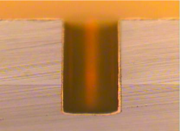
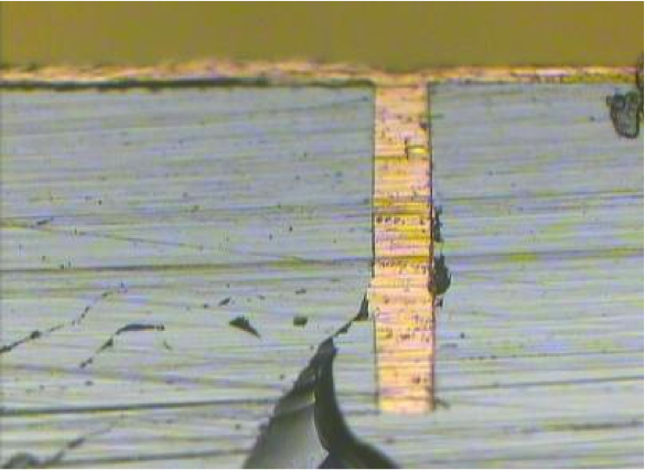
With the help of Charles Ellis in the AMNSTC, we have developed a reliable through-Si via (TSV) process that we are using in our in-house 2.5D / 3D packaging and integration. This technology uses PEALD deposited Ru seed layers and electroplated Cu TSVs.
These structures exhibit excellent filling, high aspect ratio and excellent uniformity. Current efforts are in characterizing the RF / signal integrity performance of these structures, as well as exploring integration density, reliability, forming superconducting versions, etc.

